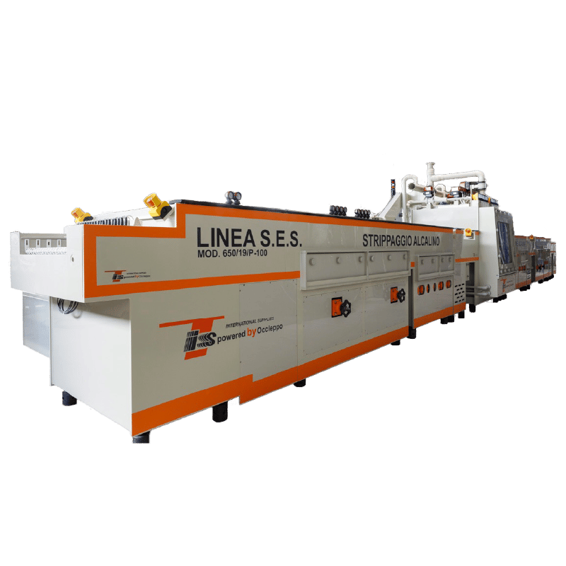

Alkaline developing systems are used to develop photosensitive layers for structuring printed circuit boards. The unexposed photoresist or solder mask on the circuit board is removed by the alkaline developer solution and the exposed copper surfaces are treated further in subsequent processes.
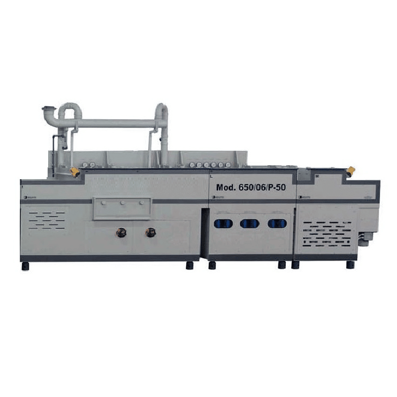
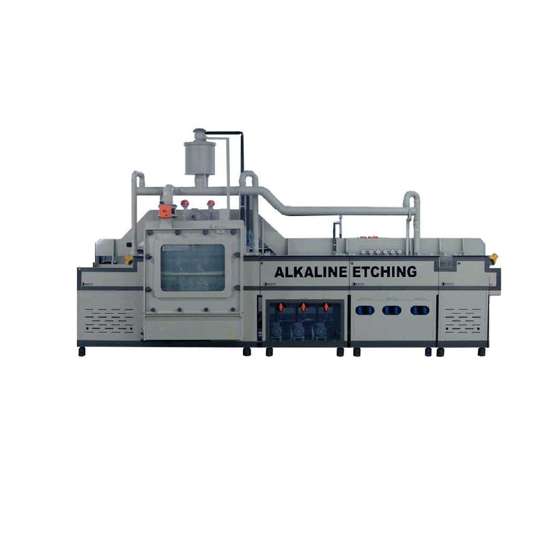
In etching systems, the exposed copper is sprayed with an alkaline or acidic etching solution, depending on the application, and removed down to the base material. This creates the conductor pattern structure, the resolution and quality of which is crucial to the overall quality of the PCB. This makes the etching process one of the most important manufacturing steps in PCB production.
Etching modules are equipped with oscillating optimised fine line nozzle bars, which are arranged lengthwise or crosswise to the transport direction to ensure a uniform etching rate. The spray pressures can be adjusted manually or via motorised valves separately for the upper and lower sides and are indicated by digital manometers.
In resist stripping systems, the developed photoresist is removed from the PCB using an alkaline solution. Resist stripping systems are used for different production processes in the manufacture of inner layers and outer layers. In the production of inner layers, the unexposed photoresist is first developed in the developer, then the exposed copper is etched down to the base material using an acidic etching medium and, in the final step, the exposed photoresist is removed again in the resist stripping system.

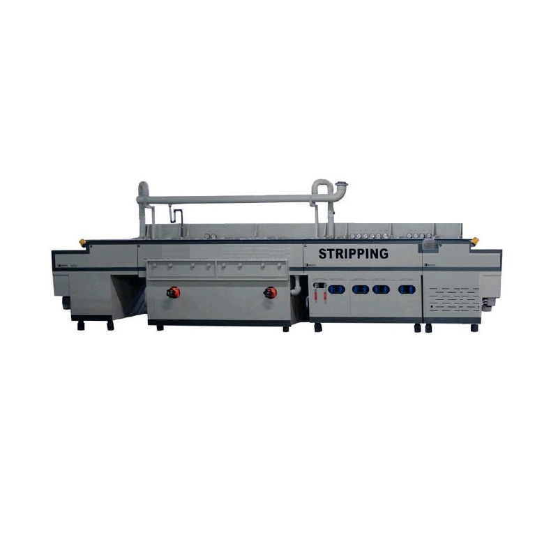
In the production of outer layers, the photoresist is used to structure an additionally deposited metal resist layer and then removed again in the resist stripping system.
The exposed copper is etched down to the base material in an alkaline etching system and the metal resist (Sn) is then removed in a tin stripping system.
Before the hot air levelling process, the copper must be pre-cleaned and activated with flux. After hot air levelling, the surface of the tinned PCBs must be completely cleaned of solder and flux. Brush modules and high-pressure rinsing support the rinsing and washing process. The post-cleaning process is usually completed by spot-free drying of the PCBs at approx. 65 °C.
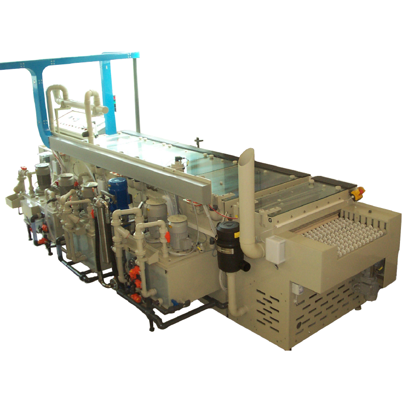
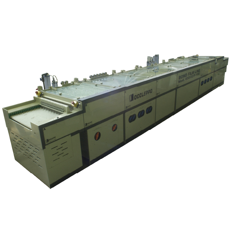
In order to eliminate the known disadvantages of black oxidation processes, process developers in PCB technology have been working on the development of alternative processes in recent years. A large number of new processes, including MecEtchBond, COBRA-Bond, Multibond, AlphaPrep and Circubond, are the result of this development work. What they all have in common is that they work in the low temperature range and improve the adhesion of copper and resin when pressing the multilayer inner layers.
Request free consultation
Our specialists will be happy to advise you on the various production processes or complete line solutions.
Request free consultation
Our specialists will be happy to advise you on the various production processes or complete line solutions.