Boardhandling
Process systems
Software solutions
Line concepts
Dispensing
Protective coating
Drying process
smartInScan – Incoming Goods
smartSCab - Storage System
Automation
Solder Paste
Solder Wire
Solder Preforms (SP)
Bar Solder
Fluxes
Stencils
Reflow Convection
Selective Soldering
Soldering Stations
Component Storage
Paste Printing
SMT Assembly
THT/OF Assembly
X-Ray Component Counting
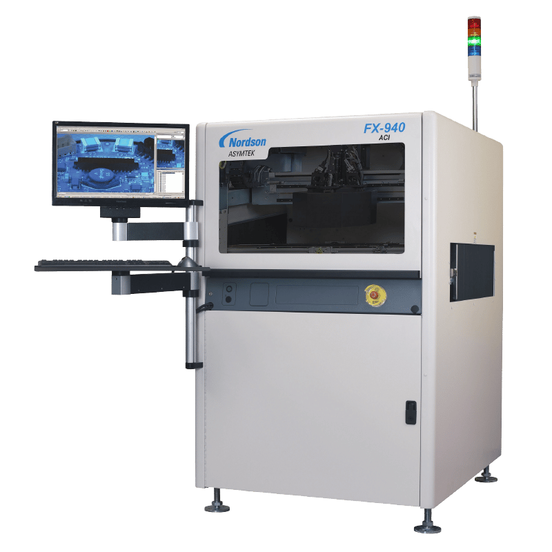
ACI
AOI
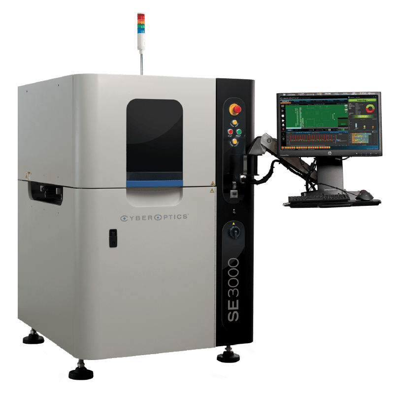
SPI
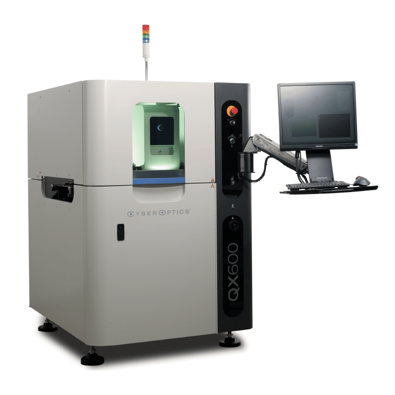
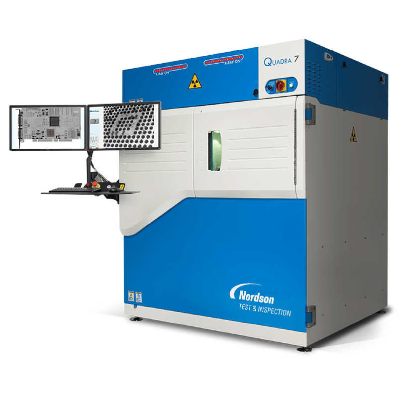
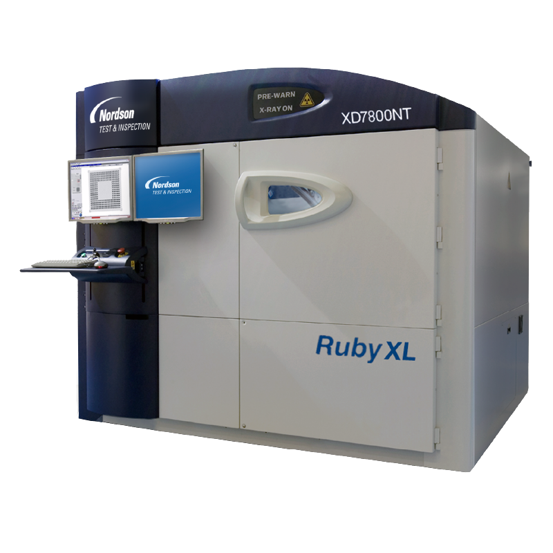
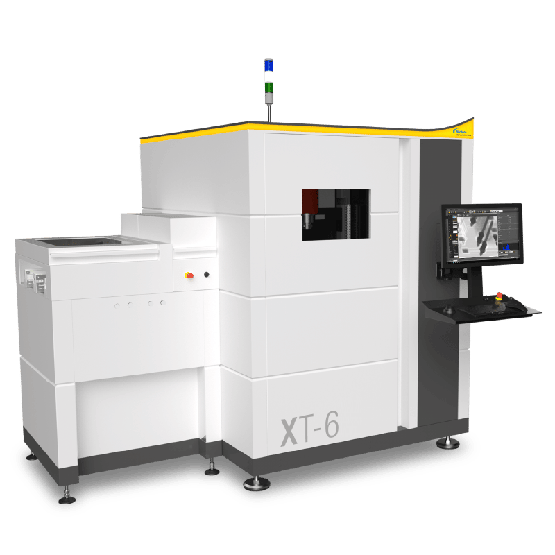
X-Ray Batch
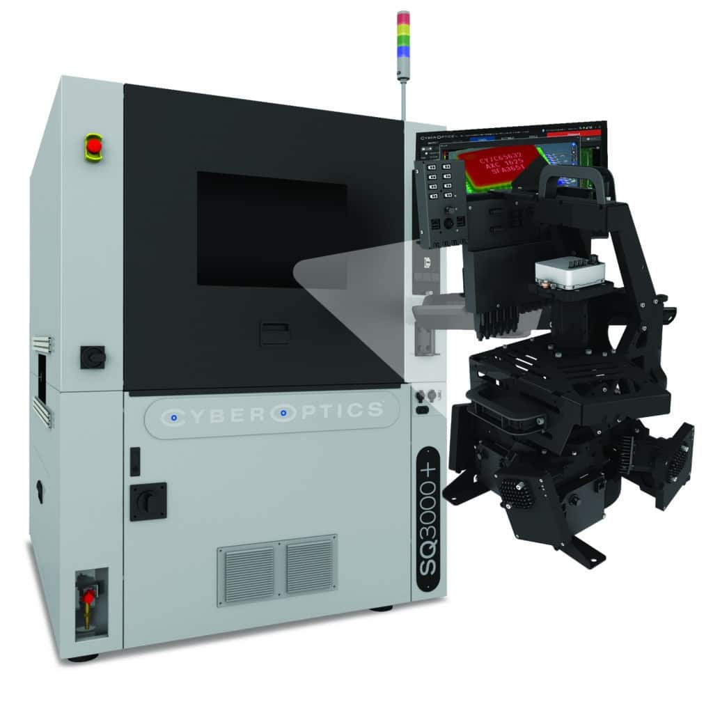
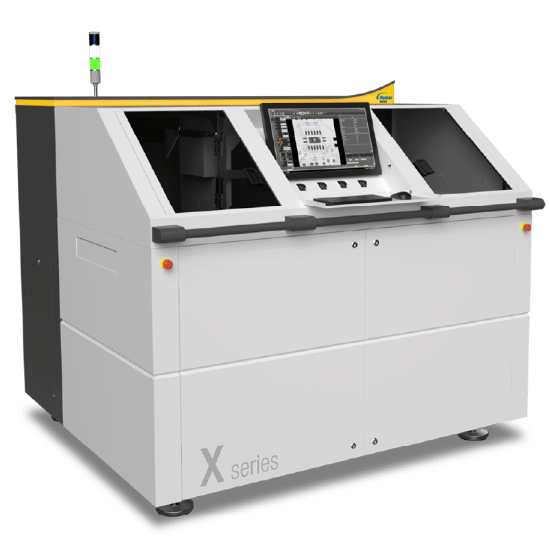
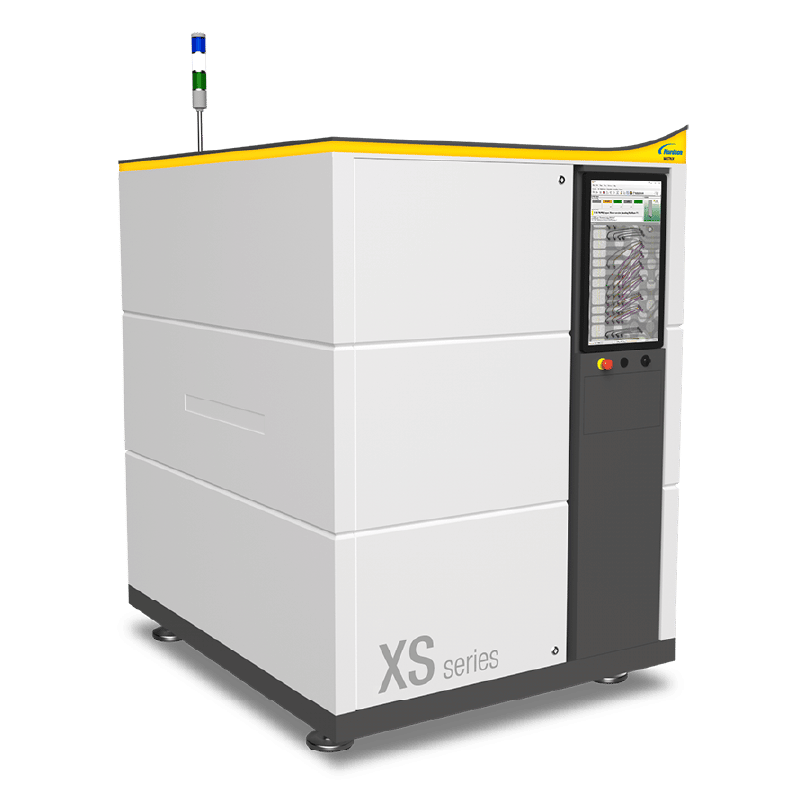
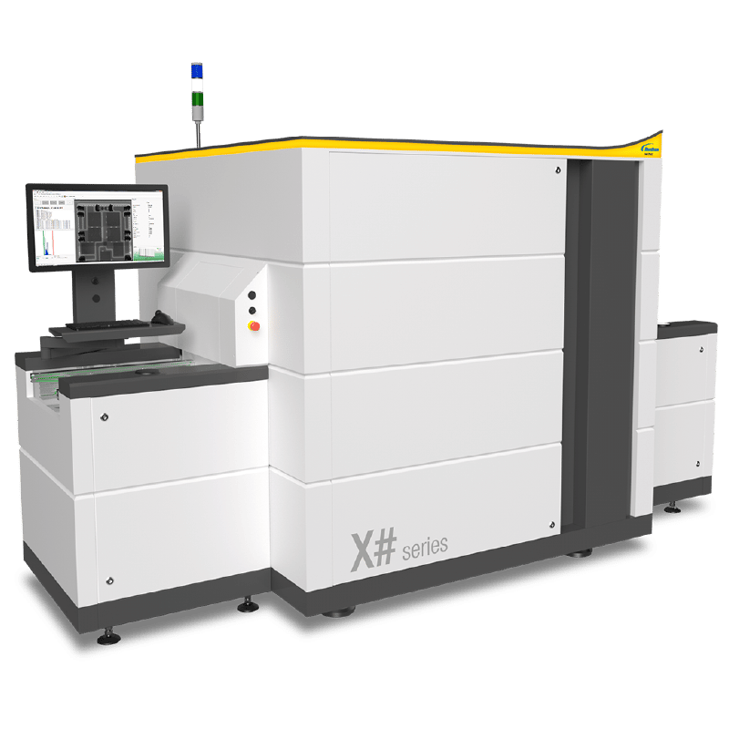
X-Ray Inline
Why smartTec?
Services
About us
Career
Request free consultation
Our specialists will be happy to advise you on the various production processes or complete line solutions.